 | –≠–ª–µ–∫—Ç—Ä–æ–Ω–Ω—ã–π –∫–æ–º–ø–æ–Ω–µ–Ω—Ç: SR037MG | –°–∫–∞—á–∞—Ç—å:  PDF PDF  ZIP ZIP |
1
SR036/SR037
06/13/02
Supertex Inc. does not recommend the use of its products in life support applications and will not knowingly sell its products for use in such applications unless it receives an adequate "products liability
indemnification insurance agreement." Supertex does not assume responsibility for use of devices described and limits its liability to the replacement of devices determined to be defective due to
workmanship. No responsibility is assumed for possible omissions or inaccuracies. Circuitry and specifications are subject to change without notice. For the latest product specifications, refer to the
Supertex website: http://www.supertex.com. For complete liability information on all Supertex products, refer to the most current databook or to the Legal/Disclaimer page on the Supertex website.
Inductorless, Dual Output Off-Line Regulators
SR036
SR037
General Description
The Supertex SR036 and SR037 are inductorless, dual output
off-line controllers. They do not require any transformers,
inductors, or high voltage input capacitors. The input voltage,
HV
IN
, is designed to operate from an unfiltered full wave
rectified 120V or 240V AC line. It is designed to control an
external N-channel MOSFET. When HV
IN
is between V
GS(th)
to
40V, where V
GS(th)
is the threshold voltage of the external
MOSFET, the external N-channel MOSFET is turned on allowing
it to charge an external capacitor connected to V
SOURCE
. An
unregulated DC voltage will develop on V
SOURCE
. Once HV
IN
is
above 45V, the N-channel MOSFET is turned off. The maximum
gate voltage for the external MOSFET is 24V. The unregulated
voltage is approximately 18V. The SR036 also provides a
regulated 3.3V whereas the SR037 provides a regulated 5.0V.
WARNING!!!
Galvanic isolation is not provided. Dangerous
voltages are present when connected to the AC line. It is
the responsibility of the designer to assure adequate
safeguards are in place to protect the end user from
electrical shock.
Features
Accepts peak input voltages up to 700V
Operates directly off of rectified 120V AC or 240V AC
Integrated linear regulator
Minimal power dissipation
No high voltage capacitors required
No transformers or inductors required
Applications
3.3V or 5.0V power supplies
SMPS house keeping power supplies
White goods
Appliances
Small off-line low voltage power supplies
Lighting controls
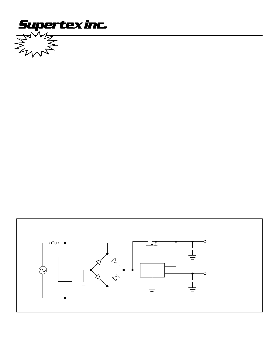
SR03x Typical Application Circuit
Sur
g
e
Pr
otection
SR036
or SR037
100
µF
1.0
µF
SR036: V
OUT
=3.3V Regulated
SR037: V
OUT
=5.0V Regulated
~
18V Unregulated
120VAC
or
240VAC
V
OUT
V
SOURCE
Gate
Demo Kit
Available
2
SR036/SR037
Absolute Maximum Ratings*
V
IN
, High Voltage Input
+700V
V
OUT
, Low Voltage Output
+6.0V
Storage Temperature
-65∞C to +150∞C
Soldering Temperature
+300∞C
Power Dissipation, MSOP-8
300mW
Power Dissipation, SO-8 slug
1.50W
* All voltages are referenced to GND.
Ordering Information
V
H
N
I
m
u
m
i
x
a
M
e
g
a
t
l
o
V
e
g
a
t
l
o
V
e
t
a
G
)
x
a
m
(
V
T
U
O
s
n
o
i
t
p
O
e
g
a
k
c
a
P
8
-
P
O
S
M
g
u
l
S
t
a
e
H
/
w
8
-
O
S
V
0
0
7
V
4
2
V
3
.
3
*
G
M
6
3
0
R
S
G
S
6
3
0
R
S
V
0
.
5
*
G
M
7
3
0
R
S
G
S
7
3
0
R
S
.
l
e
e
r
e
p
a
t
r
e
i
r
r
a
c
e
c
e
i
p
0
0
5
2
n
o
d
e
il
p
p
u
s
t
c
u
d
o
r
P
*
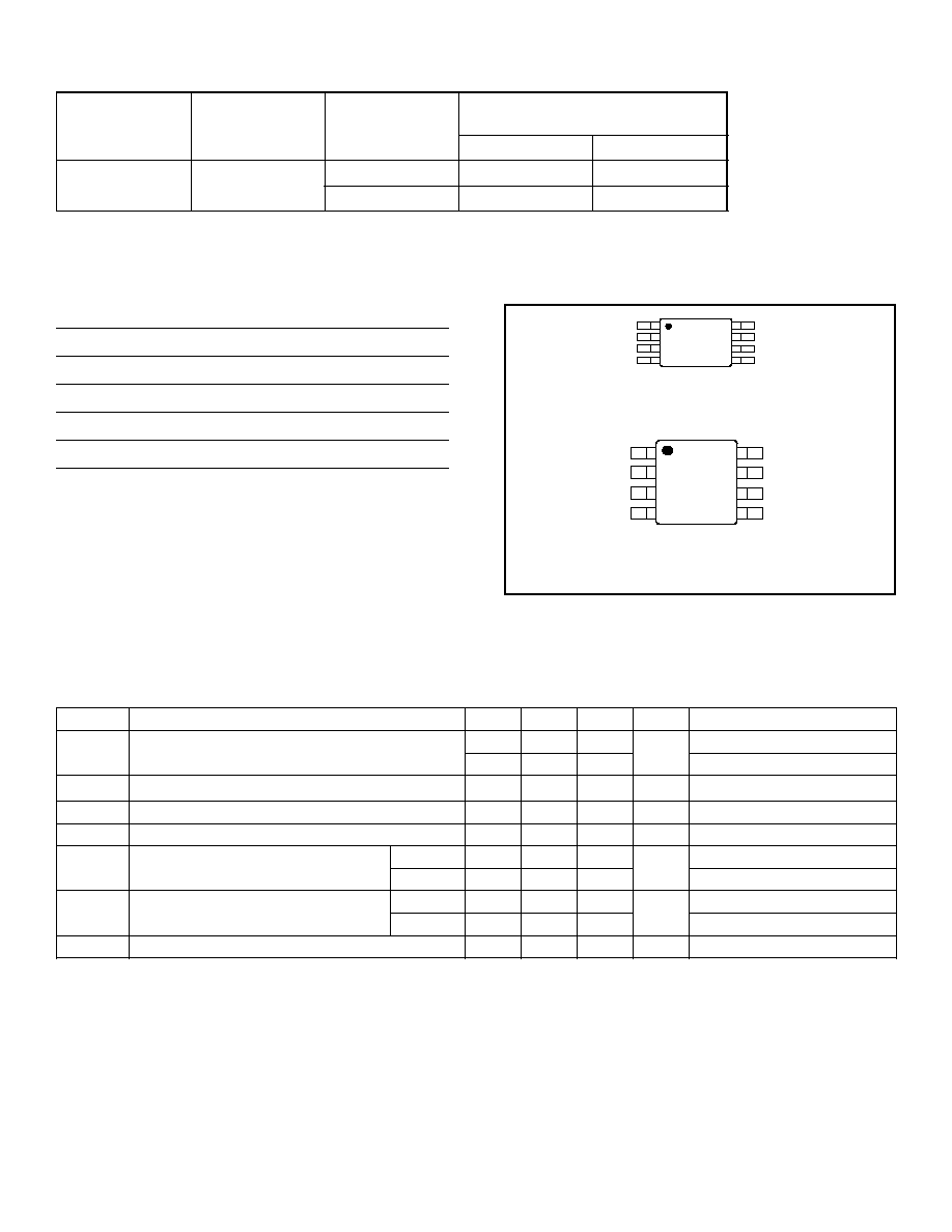
Pin Configuration
SO-8 Slug
Backside: GND
(top view)
1
2
3
4
8
7
6
5
HV
IN
Gate
N/C Source
N/C V
OUT
GND N/C
MSOP-8
(top view)
1
2
3
4
8
7
6
5
HV
IN
Gate
N/C Source
N/C V
OUT
GND N/C
Electrical Characteristics
(Over operating supply voltages unless otherwise specified, T
A
=0∞C to +125∞C)
l
o
b
m
y
S
r
e
t
e
m
a
r
a
P
n
i
M
p
y
T
x
a
M
s
t
i
n
U
s
n
o
i
t
i
d
n
o
C
V
H
N
I
e
g
a
t
l
o
v
t
u
p
n
I
0
0
7
V
e
g
a
t
l
o
v
t
n
e
i
s
n
a
r
t
k
a
e
P
7
0
4
e
g
a
t
l
o
v
C
A
d
e
i
f
i
t
c
e
r
k
a
e
P
V
H
T
V
H
N
I
d
n
u
o
r
g
o
t
d
e
ll
u
p
s
i
e
t
a
G
n
e
h
w
e
g
a
t
l
o
v
0
4
5
4
0
5
V
V
S
G
e
g
a
t
l
o
v
p
m
a
l
c
e
c
r
u
o
s
o
t
e
t
a
G
0
1
±
5
1
±
0
2
±
V
I
S
G
A
µ
0
0
1
±
=
V
E
T
A
G
e
g
a
t
l
o
v
p
m
a
l
c
d
n
u
o
r
g
o
t
e
t
a
G
8
1
0
2
4
2
V
V
T
U
O
e
h
t
r
o
f
e
g
a
t
l
o
v
t
u
p
t
u
o
d
e
t
a
l
u
g
e
R
8
-
P
O
S
M
6
3
0
R
S
7
9
.
2
0
3
.
3
3
6
.
3
V
V
E
C
R
U
O
S
I
,
V
0
1
=
T
U
O
A
m
5
1
=
7
3
0
R
S
0
5
.
4
0
0
.
5
0
5
.
5
V
E
C
R
U
O
S
I
,
V
0
1
=
T
U
O
A
m
5
1
=
V
T
U
O
8
-
O
S
e
h
t
r
o
f
e
g
a
t
l
o
v
t
u
p
t
u
o
d
e
t
a
l
u
g
e
R
g
u
l
s
t
a
e
h
h
t
i
w
6
3
0
R
S
7
9
.
2
0
3
.
3
3
6
.
3
V
V
E
C
R
U
O
S
I
,
V
0
1
=
T
U
O
A
m
0
3
=
7
3
0
R
S
5
.
4
0
0
.
5
0
5
.
5
V
E
C
R
U
O
S
I
,
V
0
1
=
T
U
O
A
m
0
3
=
q
e
r
F
y
c
n
e
u
q
e
r
f
C
A
t
u
p
n
I
0
4
0
0
1
z
H
3
SR036/SR037
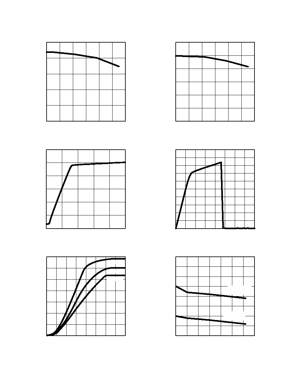
Typical Performance Curves
Gate Clamp
Temperature (
∞C)
HV
IN
(off)
Temperature (
∞C)
HV
IN
(V)
HV
IN
(V)
Vgate (V)
HV Input Current
I
IN
(
µ
A)
Load Regulation (SR037)
V
OUT
(V)
I
OUT
(mA)
Regulator Output (SR037)
V
OUT
(V)
Source Voltage (V)
Gate Voltage
HV
IN
(V)
V
Gate
(V)
-40
-10
20
50
80
110
140
0
5
10
15
20
25
-40
-10
20
50
80
110
140
0
10
20
30
40
50
60
0
5
10
15
20
25
0
1
2
3
4
5
6
0
10
20
30
40
50
60
70
80
0
2
4
6
8
10
12
14
16
18
20
0
50
100
150
200
250
300
350
400
0
300
600
900
1200
1500
1800
2100
0
5
10
15
20
25
30
35
4.65
4.70
4.75
4.80
4.85
4.90
4.95
5.00
5.05
Source=8V
25
∞C
Source=15V
25
∞C
-40
∞C
25
∞C
125
∞C
4
SR036/SR037
Applications Information
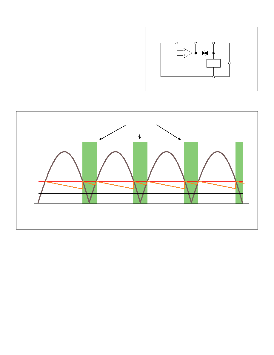
Functional Block Diagram
V
REF
CM
Reg
HV
IN
Gate
Source
GND
V
OUT
Operating Principle
The SR03x operates by controlling the conduction angle of the
external MOSFET as shown in Figure 1. When the rectified AC
voltage is below the V
TH
threshold, the pass transistor is turned
on. The pass transistor is turned off when the rectified AC is
above HV
IN(off)
. Output voltage (Vunreg) decays during the periods
when the switch is off and when the rectified AC is below the
output voltage. The amount of decay is determined by the load
and the value of C1. Since the switch only conducts with low
voltages across it, power dissipation is minimized.
Switch ON
V
TH
HV
IN
V
REG
V
UNREG
not to scale
Figure 1: Typical Waveforms
5
SR036/SR037
Applications Information, continued
220
µF
1
µF
SR036
or SR037
VN2460N8
V
UNREG
HV
IN
GND
Gate
Source
V
OUT
V
REG
I
OUT
typical 40mA
(
I
UNREG +
I
REG)
Fuse
Surge
Protection
120VAC
or
240VAC
Figure 2: Example Circuit with Enable Control
1K
TN2106K1
ON/OFF
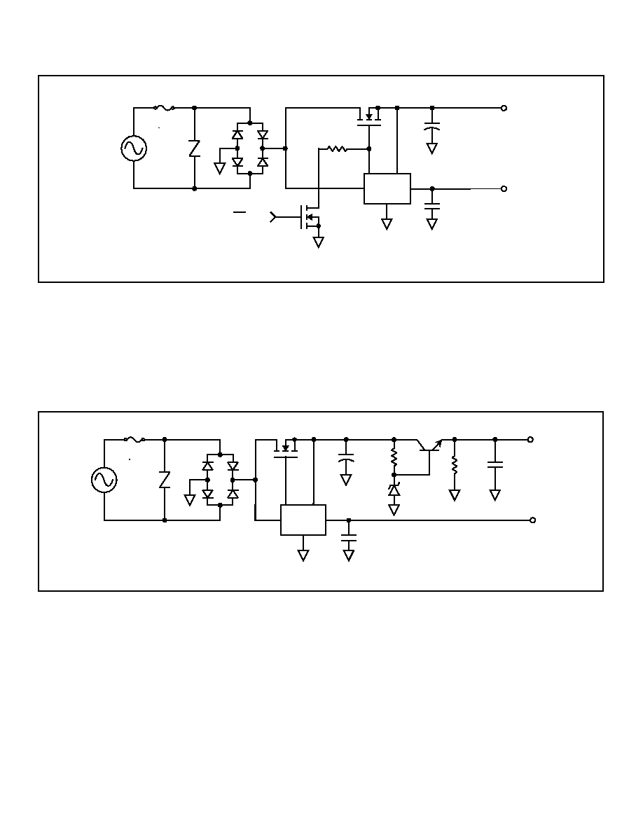
Figure 3: Generating Two Regulated Voltages
220
µF
1
µF
SR036
VN2460N8
1
µF
1M
Vz
5.6V
V
out1
=5.0V
V
out2
=3.3V
10K
120VAC
or
240VAC
Fuse
Surge
Protection
2N3904
HV
IN
GND
Gate
Source
V
OUT
Figure 2 is an example circuit using the SR036 or SR037 along
with a Supertex VN2460N8 MOSFET to generate an unregu-
lated voltage of approximately 18V and a regulated voltage of
3.3V for the SR036 or 5.0V for the SR037. The combined total
output current is typically 40mA. The TN2106K1 in series with a
1K resistor can be added for applications requiring an enable
control.
For applications requiring two regulated voltages, an inexpen-
sive discrete linear regulator can be added to regulate the
unregulated output as show in Figure 3. The discrete linear
regulator consists of a Zener diode, a resistor and a bipolar
transistor. The regulated voltage, Vout1, is determined by the
Zener diode voltage minus the base-to-emitter voltage drop of
0.6V. Figure 3 uses a 5.6V Zener diode to obtain a 5.0V output.
Different Zener diode voltages can be used to obtain different
regulated output voltages.
6
SR036/SR037
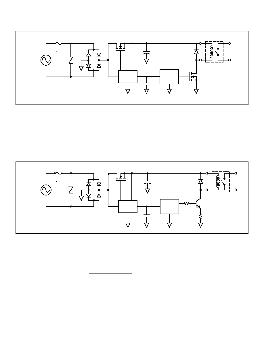
Applications Information, continued
12V Coil
Relay
220
µF
1
µF
SR036
VN2460N8
120VAC
or
240VAC
Fuse
Surge
Protection
Logic
Control
Circuit
Unregulated Voltage
3.3V
VN2110K1
1N4001
HV
IN
GND
Gate
Source
V
OUT
Figure 4: Driving 12V Relay Coils
The circuit shown in Figure 4 uses the SR036 to supply a
regulated 3.3V for the logic control circuitry while the unregu-
lated voltage is used to drive a 12V relay coil. The operating
voltage for a 12V relay coil is typically very wide and can
therefore operate directly from the unregulated line.
220
µF
1
µF
SR037
VN2460N8
120VAC
or
240VAC
Fuse
Surge
Protection
Logic
Control
Circuit
Unregulated Voltage
5.0V
100
1K
2N3904
1N4001
5V Coil
Relay
HV
IN
GND
Gate
Source
V
OUT
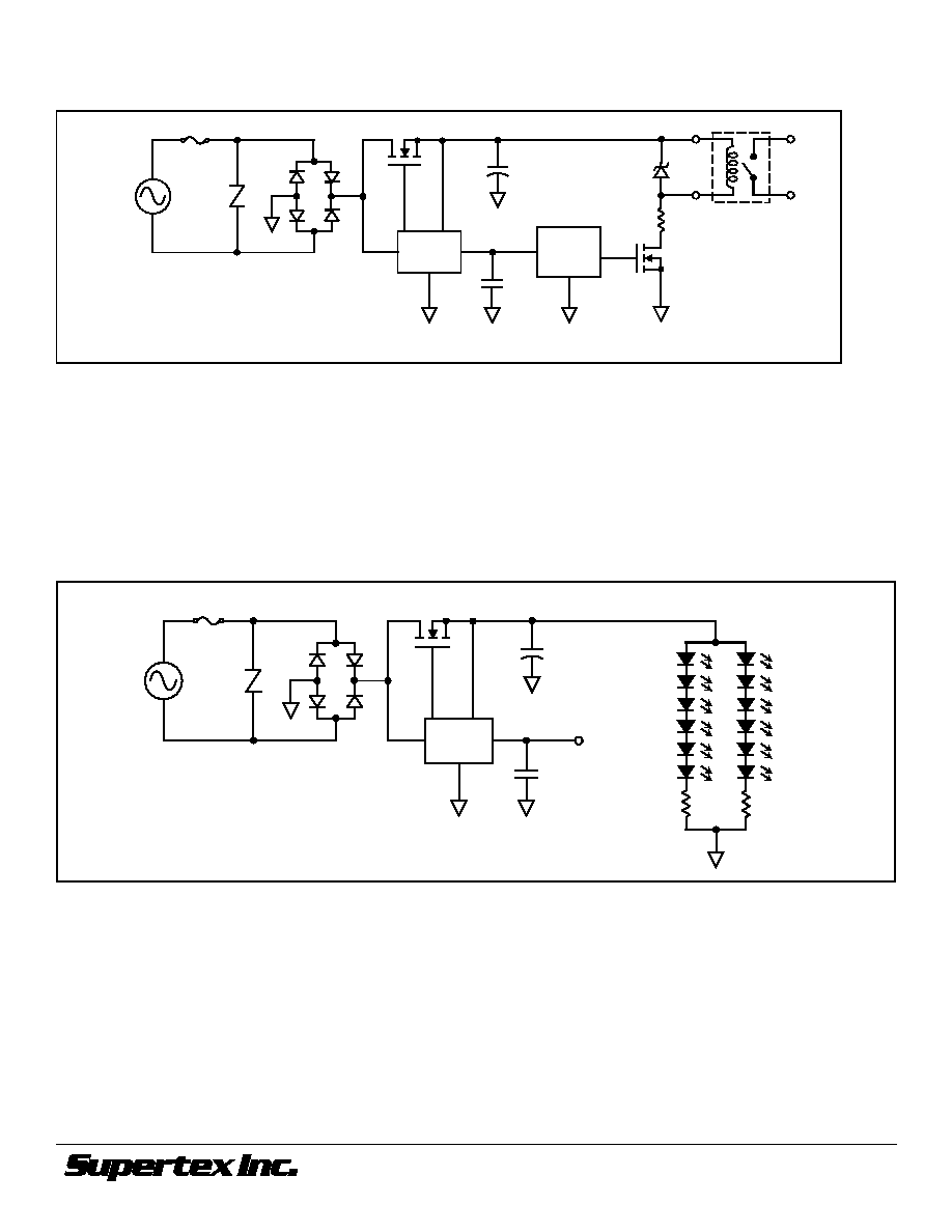
Figure 5: Driving 5V Relay Coils
The circuit shown in Figure 5 uses the SR037 to supply a
regulated 5.0V for the logic control circuitry while the unregu-
lated voltage is used to drive a 5.0V coil relay. To overcome the
voltage variation of the unregulated line, a bipolar transistor is
used to drive the coil with a constant current. The resistor value
from the emitter to ground sets the desired coil current. For an
arbitrary coil current of 40mA, the resistor value can be calcu-
lated as:
R =
5.0V -
40mA
1K - V
40mA
where V
= 0.6V and = 100
= 100
be
be
,
7
SR036/SR037
Applications Information, continued
1235 Bordeaux Drive, Sunnyvale, CA 94089
TEL: (408) 744-0100 ∑ FAX: (408) 222-4895
www.supertex.com
06/13/02rev.12
©2002 Supertex Inc. All rights reserved. Unauthorized use or reproduction prohibited.
220
µF
1
µF
SR037
VN2460N8
120VAC
or
240VAC
Fuse
Surge
Protection
Logic
Control
Circuit
Unregulated Voltage
5.0V
5V Coil
Relay
Vz
5.1V
HV
IN
GND
Gate
Source
V
OUT
Figure 6: Driving 5V Relay Coils with Zener Diode Clamp
The circuit shown in Figure 6 uses the SR037 to supply a
regulated 5.0V for the logic control circuitry. A 5.1V Zener diode
is used in parallel with the 5.0V relay coil to ensure that the relay
coil's maximum operating voltage is not exceeded. The Zener
diode also acts as the catch diode when the coil is switched to the
off state. An external series resistor is used to limit the amount
of Zener current.
220
µF
1
µF
SR036 or
SR037
TN2425N8
120VAC
Fuse
Surge
Protection
330
330
Unregulated Voltage
HV
IN
GND
Gate
Source
V
OUT
Figure 7: Driving LEDs from 120VAC
V
REG
The circuit shown in Figure 7 uses the SR036 or SR037 to drive
12 high efficient red LEDs from a 120V AC line. The average LED
current is approximately 20mA.